
In the fast-paced world of semiconductor manufacturing, precision and accuracy are paramount. Ensuring the reliability and performance of semiconductor devices demands meticulous testing processes, and at the heart of these procedures lies the unassuming yet crucial component: the test wafer. In this comprehensive guide, we will delve into the intricate world of test wafers, exploring their importance, types, selection criteria, handling, equipment, experimental setup, data analysis, troubleshooting, maintenance, real-world applications, and future trends.
Table of Contents
Importance and Purpose
Test wafers are the unsung heroes of semiconductor testing. These wafer-sized substrates, typically made of silicon, mimic the actual manufacturing process and allow for comprehensive testing of various parameters, ensuring the quality and performance of semiconductor devices. Their significance lies in their ability to represent real-world conditions accurately. This is achieved by replicating the materials, structures, and processes used in production wafers, making them invaluable for process development, equipment calibration, and quality control.
Understanding Materials and Types
They come in a variety of materials, with silicon being the most common due to its compatibility with semiconductor manufacturing processes. Other materials, like gallium arsenide and silicon carbide, cater to specific applications. They can also vary in terms of thickness, size, and the types of structures they feature, such as microelectromechanical systems (MEMS) or integrated circuits (ICs).
Selecting the Right Test Wafer for Your Application
Choosing the appropriate one is a critical decision that directly impacts the success of your testing endeavors. Factors to consider include material compatibility, wafer specifications, and the specific parameters you need to test. Understanding your application’s requirements and the compatibility with your testing equipment is essential to ensure accurate results.
For instance, if your semiconductor device operates in high-temperature conditions, selecting the one with a thermal expansion coefficient similar to your production wafers is crucial to avoid measurement errors caused by thermal stress. Similarly, if you’re testing MEMS devices, opt for them that replicate the MEMS structures accurately.
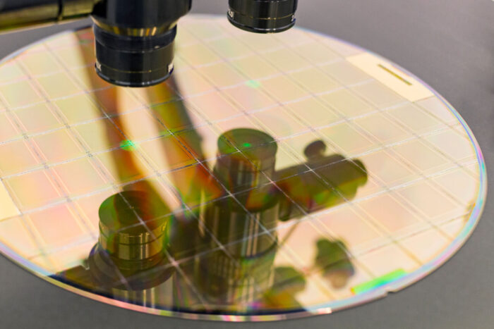
Proper Handling and Storage
The proper handling and storage are crucial to maintaining their integrity and reliability. Contaminants, such as dust particles or fingerprints, can lead to erroneous test results. Storing wafers in a clean, controlled environment with suitable packaging is essential to preserve their quality.
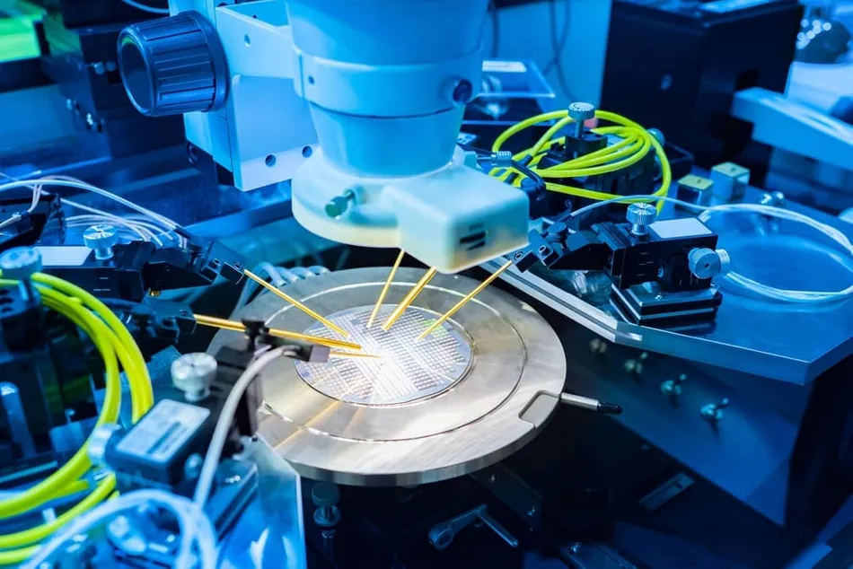
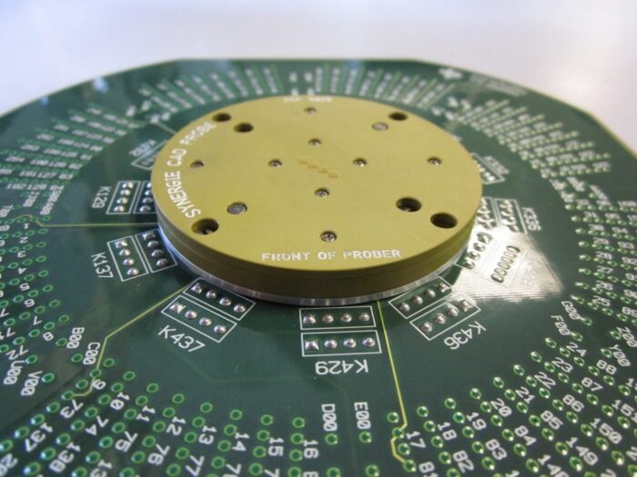
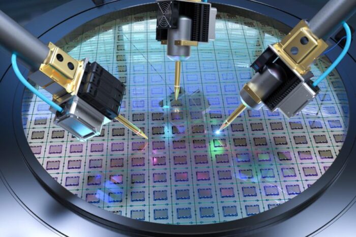
Essential Equipment for Testing
To conduct accurate tests, you need the right equipment. This includes test systems, probe stations, and specialized testing instruments tailored to your specific application. Investing in high-quality equipment is essential to achieving consistent and reliable results.
Probe stations, for instance, are essential for making electrical contact with them. These stations come in various configurations, such as manual or automated, and can be equipped with features like precise positioning and temperature control. The choice of probe station depends on the complexity of your testing requirements.
Setting Up Experiments for Accuracy
Creating precise test protocols and experimental setups is pivotal in obtaining accurate results. Ensure that your experiments are well-designed and properly calibrated, and that they are handled with care during testing. Consistency in your testing procedures is key to reducing variability and increasing the reliability of your results.
Calibration is a critical step in the setup process. Regularly calibrate your testing equipment to maintain measurement accuracy. Additionally, establish a robust methodology for aligning and probing them to ensure consistent contact and measurement repeatability.
Data Analysis Techniques for Results

Collecting data is one thing, but extracting meaningful insights from it is another. Employ advanced data analysis techniques, including statistical methods and data visualization tools, to interpret your results effectively. These techniques can uncover hidden trends, anomalies, and correlations that might otherwise go unnoticed.
Troubleshooting Common Issues
During testing, sample transistors may have a range of problems, including flaws, contamination, or measurement mistakes. To quickly discover and resolve these problems, save downtime, and ensure the dependability of your testing procedures, you must have troubleshooting abilities.
Best Practices for Maintaining Quality
To maximize the lifespan and effectiveness adhere to best practices for their maintenance. Regularly inspect, clean, and store them properly. Implement a robust quality control process to ensure that they remain consistent and reliable over time.
Routine inspections should include visual examinations, measurements of critical parameters, and thorough cleanliness checks. Implement a documentation system to track the history and condition of each one, facilitating traceability and ensuring the validity of test results.
Case Studies: Successful Applications
To illustrate the real-world impact of mastering test wafers, we present a series of case studies highlighting successful applications across various industries. From semiconductor manufacturing to MEMS development and beyond, these examples showcase the versatility and significance of achieving groundbreaking results.
Case Study 1: Semiconductor Yield Improvement
A semiconductor manufacturer was facing low yield rates in their production process. By using them to identify process variations and optimize equipment settings, they significantly increased yield, resulting in substantial cost savings and improved product quality.
Case Study 2: MEMS Sensor Development
In the field of MEMS sensor development, they enabled researchers to experiment with various sensor designs and materials. This iterative process allowed them to create highly sensitive and reliable sensors for applications in automotive, aerospace, and healthcare.
Case Study 3: Photovoltaic Cell Efficiency
A solar panel manufacturer utilized test wafers to develop and test new photovoltaic cell designs. Through rigorous testing and analysis, they improved cell efficiency, leading to higher energy output and greater competitiveness in the renewable energy market.
Conclusion and Future Trends
As technology advances, so do the demands on test wafers. In conclusion, mastering test wafers is not just about current best practices but also about staying ahead of future trends. As the semiconductor industry continues to evolve, it will play an increasingly pivotal role in enabling innovation and ensuring the reliability of cutting-edge devices. Stay tuned for emerging technologies and techniques in testing that will shape the future of semiconductor manufacturing.
In this comprehensive guide, we’ve journeyed through the world of test wafers, from their fundamental importance to advanced techniques and real-world applications. Armed with this knowledge, you’re well-equipped to tackle the challenges of semiconductor testing with confidence and precision. As technology continues its relentless march forward, mastering it will remain a cornerstone of excellence in the semiconductor industry.